
Research · spintronics
Interdiffusion at a 2D metal/semiconductor contact, and what it does to device performance
Cooling a finished device and warming it up again moves its magnetic coupling by a factor of five, with nothing about the fabrication changed.
The short version
Two magnetic crystals stacked together are usually assumed to sit side by side without mixing. If the contact between them changes with nothing more than cooling and warming, a device's behaviour depends on its thermal history and not only on how it was made. That is a reliability question for anything built on such interfaces.
The stack pairs the metallic ferromagnet Fe3GeTe2 (FGT) with MnPS3, a compensated antiferromagnet whose interface spins should cancel.
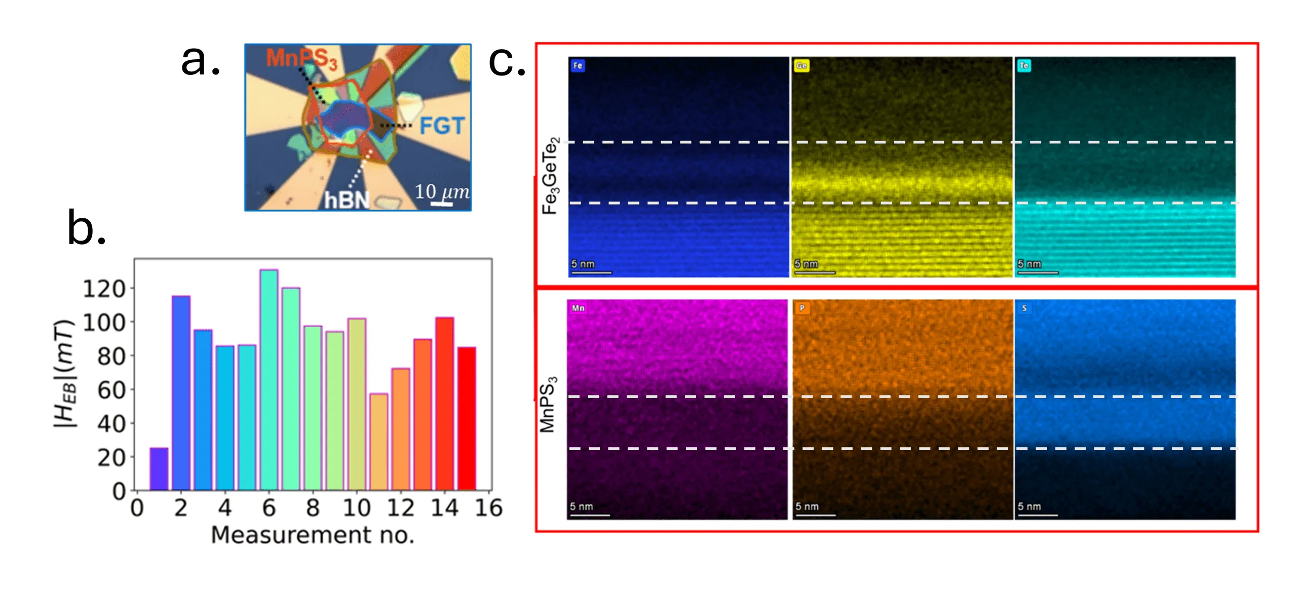 Fifteen cooling cycles on one device move its bias by a factor of five, and the elemental maps show the intermixed region that goes with it. Adapted from Advanced Materials 36, 2403685 (2024), © Wiley-VCH GmbH.
How
- Located the source of the bias by scanning nitrogen-vacancy magnetometry: below 40 K MnPS3 undergoes a spin reorientation that leaves a small uncompensated moment, and the bias follows it.
- Cycled the same device between cold and warm and measured the bias each time, a swing approaching 1000% across devices with fabrication unchanged.
- Traced the drift to the interface by cross-sectional electron microscopy with elemental mapping on cycled and uncycled lamellae. The link is correlative: no single interface was watched continuously.
Shared first authorship with Aravind Puthirath Balan. Published in Advanced Materials 36, 2403685 (2024), 10.1002/adma.202403685. The analysis code is public on GitHub as EB-in-FGT-MPS-vdW-heterostructure.