A near-monochrome collage of seven laboratory photographs cut into diagonal panels: a cryostat and vacuum chamber trailing cabling and steel flanges; an optical table with posts, a glowing lamp and a circuit board; a bright ring of light seen through a dark chamber viewport; a chamber interior with a finned copper disc, translation stages and stepper motors; a rack of long cryostat probe inserts with stacked baffles; a vacuum chamber wrapped in aluminium foil with pneumatic valves; and a chamber with a brilliant glowing plume beneath a circular electrode.

Research

I build devices out of magnetic crystals only a few atomic layers thick, then measure what happens at the interface between them. Each theme below asks a different question of the same underlying physics: how two ultra-thin magnetic materials influence each other once you stack them together. Every device is built from exfoliating the crystals and dry-transferring them into stacks on sputtered thin-films pattenerd into device structure through lithography and etching and characterized through cryogenic transport, magnetometry and nanoscale magnetic imaging, with electron microscopy run through partner institutes.

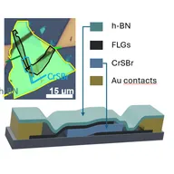
An optical micrograph of the junction with the h-BN, few-layer graphene and CrSBr flakes outlined in yellow, black and blue against a 15 micrometre scale bar, above a three-dimensional cutaway schematic of the same stack showing teal h-BN over black graphene electrodes, a blue CrSBr layer and gold contacts on a dark substrate, with a colour key naming each material.

Bias-tunable magnetoresistance in a CrSBr junction, and the mechanism behind it

spintronics · magnetoresistance · CrSBr

Devices that read out magnetic state electrically normally need two magnetic electrodes with an insulator between them. This one has no magnetic electrodes at all: the magnetism sits in the insulating layer itself, and the resistance still changes by a factor of four and a half depending on how that layer's internal magnetic order is arranged. The size of the effect is set by the operating voltage, and we identify what causes it.

A colour-coded magnetic induction map of the device cross-section: concentric contour loops in green, red and violet on a dark field, crossed by two horizontal orange dashed lines marking the layer interfaces.

Exchange bias between magnets pointing at right angles, and the domain structure behind it

spintronics · exchange bias · van der Waals magnets

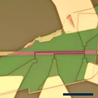
Magnetic coupling across an interface is usually described between two magnets that share an axis. This work paired two whose preferred directions are perpendicular to each other, showed they still couple strongly enough to bias one another, and then imaged the magnetic structure inside the device to explain how. The direction of the effect is set by a magnetic-field pulse at operating temperature, without cooling the device through any transition.

An optical micrograph of the device: a magenta strip running horizontally across a green flake, with pale gold contacts fanning out below it and a dark scale bar at bottom right.

Magnon spin valve in Pt / CrPS4 / Pt

spintronics · magnon transport · antiferromagnets

This device sandwiches a magnetic semiconductor between two platinum layers: one platinum layer injects a wave of the material's magnetism, called a magnon, and the second layer reads it out on the other side. Switching the orientation of the magnetic layer in the middle turns that signal on or off, like a valve. This is an earlier-stage, ongoing project, and this page is a short summary rather than a full write-up.

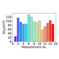
A bar chart of exchange bias magnitude in millitesla against measurement number, fifteen rainbow-coloured bars ranging from about 25 to 130 millitesla with no monotonic trend.

Interdiffusion at a 2D metal/semiconductor contact, and what it does to device performance

spintronics · exchange bias · van der Waals magnets

Two magnetic crystals stacked together are usually assumed to sit side by side without mixing. Here, simply cooling the device down and warming it up again moves atoms across that contact, closes the gap between the layers, and changes the strength of the magnetic coupling by around a factor of ten. Nothing about the fabrication changed; only the thermal history did.

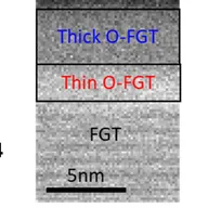
A greyscale cross-sectional electron micrograph with a 5 nm scale bar, showing three stacked bands outlined in black and labelled thick O-FGT, thin O-FGT and FGT.

Surface oxidation as the dominant source of exchange bias

spintronics · exchange bias · van der Waals magnets

Fe3GeTe2, one of the magnetic crystals in this stack, grows a thin rust layer within half an hour of air exposure. Rather than treating that layer as damage, we measured what it does, and found it takes over the magnetic coupling between the two crystals and can reverse its direction. It is a reminder that at these thicknesses an unintended interface layer is not a defect at the edge of the device, it is the device.