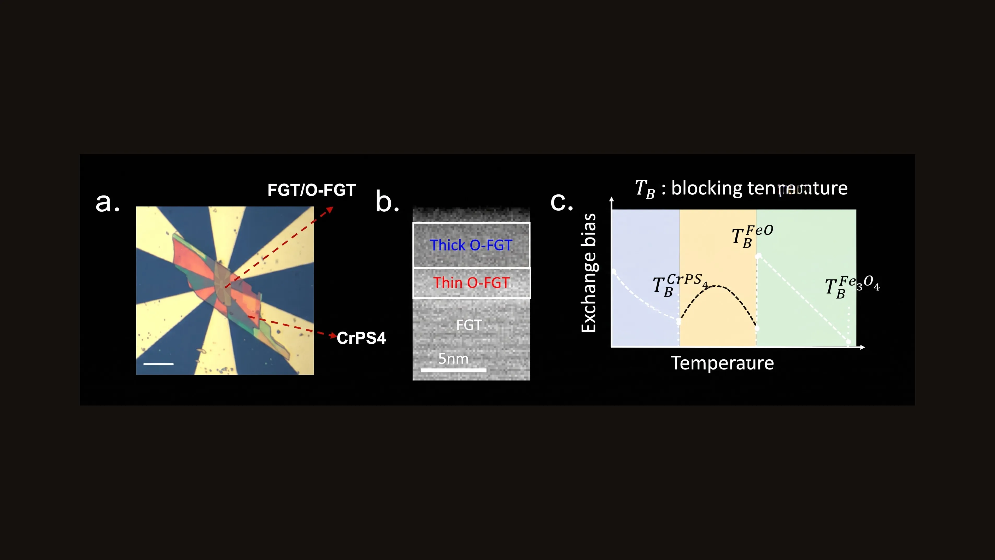
Research · spintronics
Surface oxidation as the dominant source of exchange bias
The rust layer everyone treats as damage turns out to run the magnetic coupling, and can reverse its direction.
The short version
Fe3GeTe2, one of the magnetic crystals in this stack, grows a thin oxide layer within half an hour of air exposure, and that layer is usually treated as damage. At these thicknesses an unintended interface layer can be a large part of the device, so what it does to the magnetic coupling between the two crystals had to be measured.
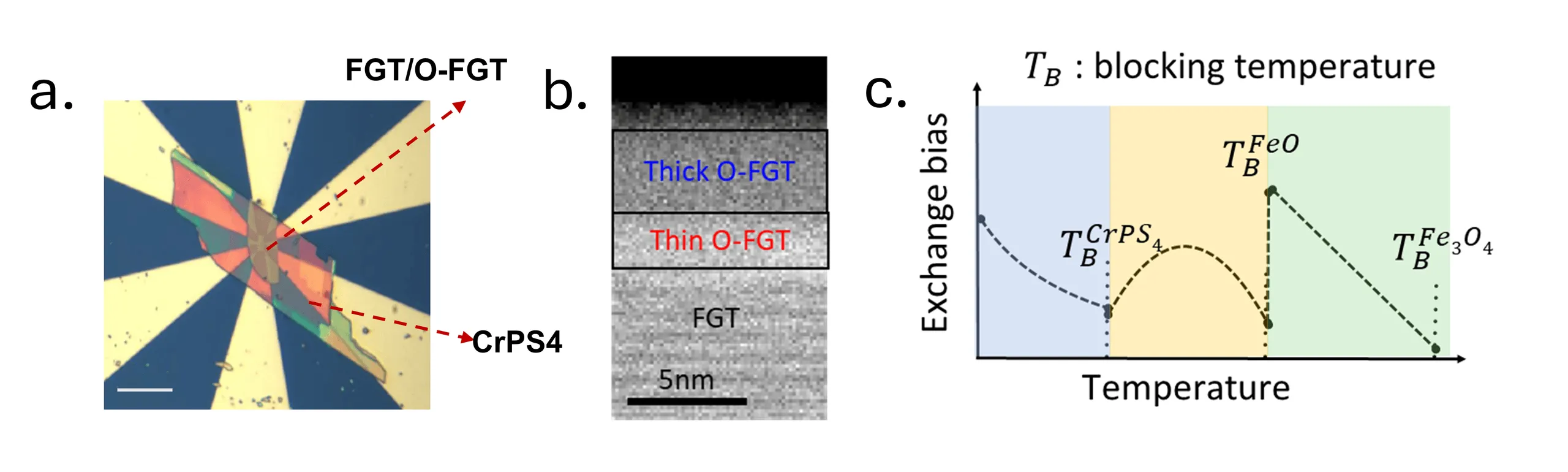 Each magnetic phase in the stack stops pinning at its own blocking temperature, which is why the bias is non-monotonic in temperature. Adapted from ACS Nano 18, 8383–8391 (2024), © American Chemical Society.
How
- Let the Fe3GeTe2 (FGT) oxidise on purpose and measured exchange bias across the FGT/CrPS4 stack against a pristine, hBN-capped control device.
- Resolved the native oxide by cross-sectional electron microscopy with elemental spectroscopy (STEM-EELS) and X-ray photoelectron spectroscopy (XPS): two magnetically ordered sublayers, which explain the bias minima near 20 K and 70 K.
- Set the sign with a ±1 T preset at fixed temperature, with no field cooling.
- Stated the limits: the layer-by-layer assignment rests on a three-region spin model rather than depth-resolved magnetometry, and the effect is cryogenic.
Shared first authorship with Aravind Puthirath Balan. Published in ACS Nano 18, 8383–8391 (2024), 10.1021/acsnano.3c13034. The analysis code is public on GitHub as EB-in-FGT-OFGT-CrPS4-vdW-heterostructure.