Research · spintronics
Bias-tunable magnetoresistance in a CrSBr junction, and the mechanism behind it
A magnetic tunnel junction with no magnetic electrodes at all, switching its resistance by 350%.
The short version
Devices that read out magnetic state electrically normally need two magnetic electrodes with an insulator between them. Junctions whose insulating barrier is itself magnetic show a distinctive M-shaped dependence on operating voltage, and the literature explains it in several incompatible ways. Without the mechanism there is no way to design for the effect.
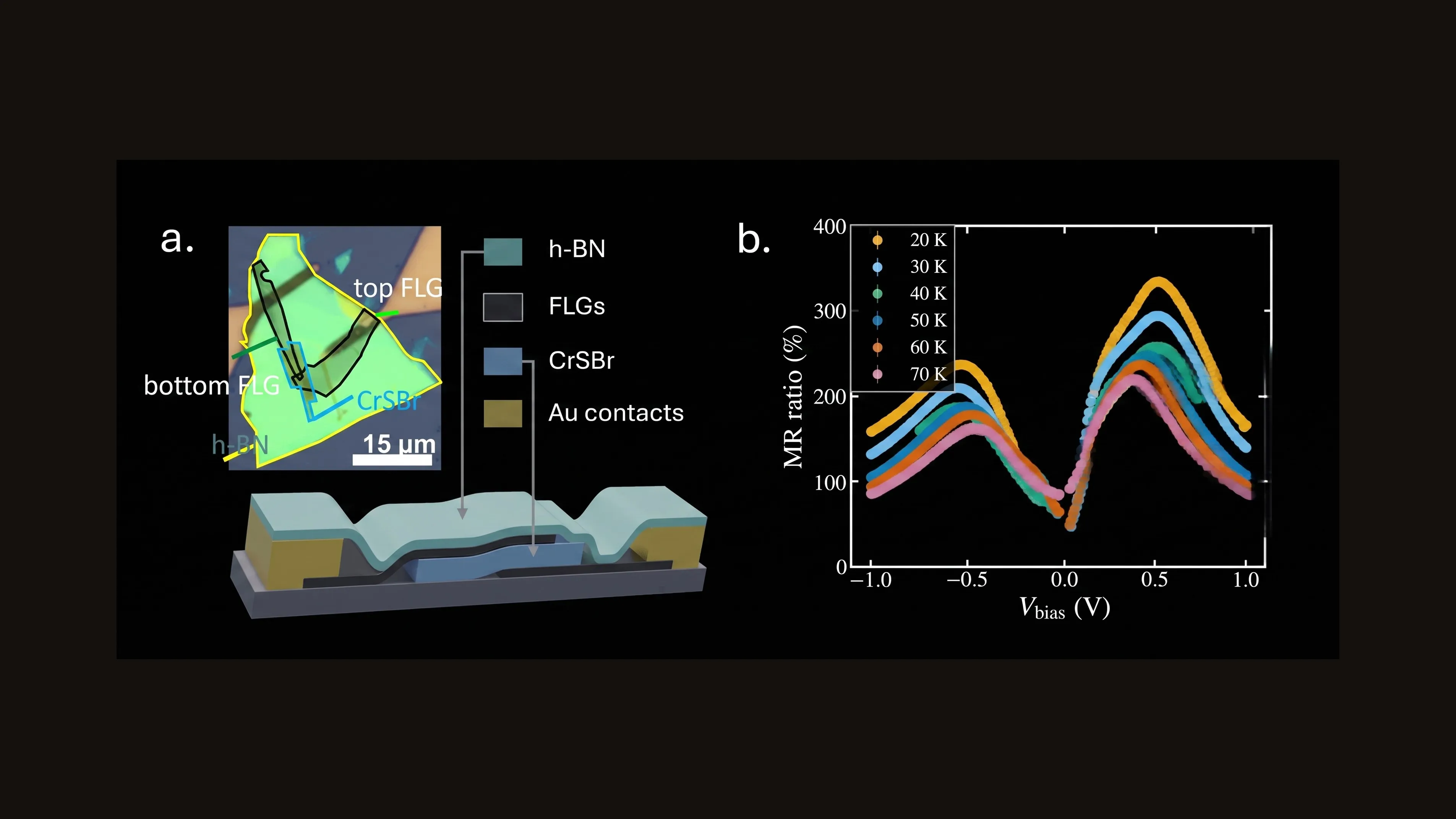
Both electrodes are non-magnetic few-layer graphene. The magnetism sits in the 12 nm CrSBr barrier between them, whose own antiferromagnetic order sets the barrier height.
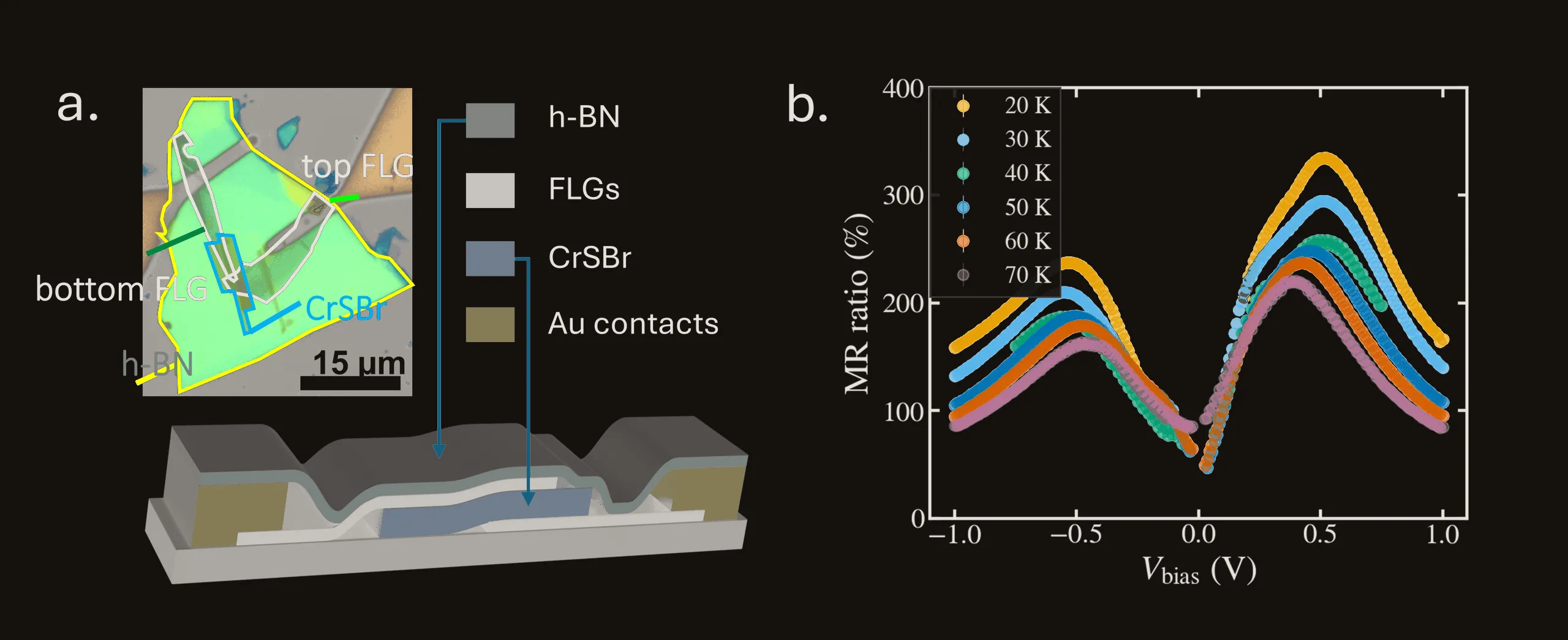 The two maxima near ±0.5 V are the field-emission onsets of the two magnetic configurations; they merge and vanish above about 90 K.
How
- Rotated the layer magnetisations continuously with a hard-axis field, instead of only switching between the two collinear states. The band-edge offset moves linearly with cos(θ/2), the first-order signature of spin-dependent interlayer hybridisation; the Jullière model and a spin-filter projection both predict a quadratic dependence.
- Built the measurement chain for the high-impedance regime, where the junction's resistance rivals the wiring's leakage paths: a liquid-helium vector cryostat with an electrometer and a Keithley source-measure unit, every cable qualified by time-domain reflectometry on a vector network analyser, single-point grounding and end-to-end shielding against ground loops, parasitic cable capacitance and radio-frequency pickup.
- Ran acquisition and per-run metadata capture on CryoSoft, with a reproducible per-project analysis workflow on top.
- Kept the energy scale honest: it rests on an empirical bias-to-energy calibration, so it is compared on scale rather than treated as exact.
Shared first authorship with Sadeed Hameed, who fabricated the van der Waals stack by exfoliating the flakes and assembling the junction. I built the measurement chain and its protocol and worked with him on the analysis pipeline; the band-structure interpretation came from a first-principles collaboration. Fabrication and metrology are under Methods. Preprint, not yet peer-reviewed: arXiv:2608.11389.