Research · spintronics
Magnon spin valve in Pt / CrPS4 / Pt
Magnon transport through an antiferromagnet, blocked or allowed by a magnetic field.
The short version
This device sandwiches a magnetic semiconductor between two platinum layers: one platinum layer injects a wave of the material's magnetism, called a magnon, and the second reads it out on the other side. Switching the orientation of the magnetic layer in the middle turns that signal on or off, like a valve. Whether magnons cross at all is decided by the platinum/CrPS4 interfaces.
An ongoing project since 2024 in the Kläui Lab at JGU Mainz.
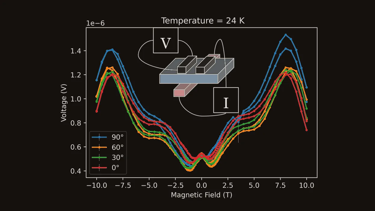
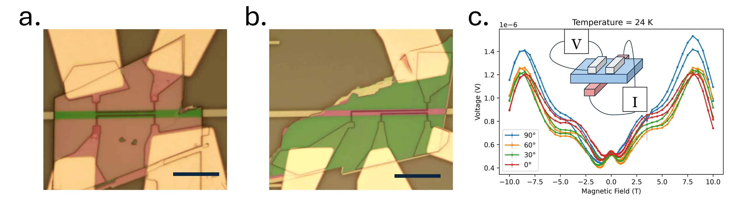 At 24 K the detected signal depends on how the field is oriented relative to the crystal, with maxima near ±8 T.
How
- Injected magnons two ways from the bottom platinum layer, thermally by the spin Seebeck effect and electrically by the spin Hall effect, and detected them in the top layer by the inverse spin Hall effect. The valve state is set by orienting the CrPS4 antiferromagnet in an applied field.
- Assembled the stack in a glove box, because CrPS4 degrades in air: flakes exfoliated from a bulk crystal and placed on sputter-deposited platinum by polymer dry transfer. Geometry by electron-beam lithography, contact pads by optical lithography, patterning by ion-beam etching, resist removal by oxygen-plasma ashing.
- Checked every device by in-house SEM and EDX before it reaches a cryostat, as the structural and compositional baseline for the handover from fabrication to measurement.
- Brought the interface recipe from my visiting-researcher year, 2021 to 2022, which characterised two routes across several deposition and transfer conditions: platinum deposited onto exfoliated CrPS4, and CrPS4 transferred onto pre-deposited platinum.
The fabrication chain is shared with the exchange-bias projects and described under Methods. Under development.